- 您现在的位置:买卖IC网 > Sheet目录3890 > PIC18C858T-I/PT (Microchip Technology)IC MCU OTP 16KX16 CAN 80TQFP
2000 Microchip Technology Inc.
Advanced Information
DS30475A-page 103
PIC18CXX8
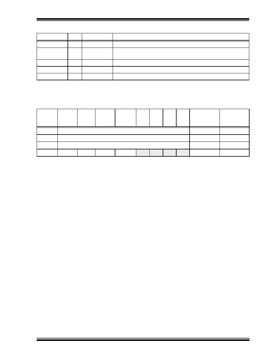
TABLE 8-13:
PORTG FUNCTIONS
Note:
Refer to "CAN Module", Section 17.0 for usage of CAN pin functions.
TABLE 8-14:
SUMMARY OF REGISTERS ASSOCIATED WITH PORTG
Name
Bit#
Buffer Type
Function
RG0/CANTX0
bit0
ST
Input/output port pin or CAN bus transmit output.
RG1/CANTX1
bit1
ST
Input/output port pin or CAN bus complimentary transmit output or CAN
bus bit time clock.
RG2/CANRX
bit2
ST
Input/output port pin or CAN bus receive input.
RG3
bit3
ST
Input/output port pin.
RG4
bit4
ST
Input/output port pin.
Legend: ST = Schmitt Trigger input
Name
Bit 7
Bit 6
Bit 5
Bit 4
Bit 3
Bit 2
Bit 1
Bit 0
Value on:
POR,
BOR
Value on all
other
RESETS
TRISG
PORTG Data Direction Control Register
---1 1111
PORTG
Read PORTG pin / Write PORTG Data Latch
---x xxxx
---u uuuu
LATG
Read PORTG Data Latch/Write PORTG Data Latch
---x xxxx
---u uuuu
CIOCON
TX1SRC
TX1EN
ENDRHI
CANCAP
—
0000 ----
Legend: x = unknown, u = unchanged
发布紧急采购,3分钟左右您将得到回复。
相关PDF资料
PIC18C658T-I/PT
IC MCU OTP 16KX16 CAN 64TQFP
PIC16LC717T-E/SS
IC MCU OTP 2KX14 A/D PWM 20SSOP
PIC16LC771T/SO
IC MCU OTP 4KX14 A/D PWM 20SOIC
PIC16LC771T-E/SO
IC MCU OTP 4KX14 A/D PWM 20SOIC
PIC16C771T-E/SO
IC MCU OTP 4KX14 A/D PWM 20SOIC
PIC16LC770T/SS
IC MCU OTP 2KX14 A/D PWM 20SSOP
PIC16LC717T-I/SO
IC MCU OTP 2KX14 A/D PWM 18SOIC
PIC16LC771T/SS
IC MCU OTP 4KX14 A/D PWM 20SSOP
相关代理商/技术参数
PIC18F1220-E/ML
功能描述:8位微控制器 -MCU 4KB 256 RAM 16 I/O RoHS:否 制造商:Silicon Labs 核心:8051 处理器系列:C8051F39x 数据总线宽度:8 bit 最大时钟频率:50 MHz 程序存储器大小:16 KB 数据 RAM 大小:1 KB 片上 ADC:Yes 工作电源电压:1.8 V to 3.6 V 工作温度范围:- 40 C to + 105 C 封装 / 箱体:QFN-20 安装风格:SMD/SMT
PIC18F1220-E/P
功能描述:8位微控制器 -MCU 4KB 256 RAM 16 I/O RoHS:否 制造商:Silicon Labs 核心:8051 处理器系列:C8051F39x 数据总线宽度:8 bit 最大时钟频率:50 MHz 程序存储器大小:16 KB 数据 RAM 大小:1 KB 片上 ADC:Yes 工作电源电压:1.8 V to 3.6 V 工作温度范围:- 40 C to + 105 C 封装 / 箱体:QFN-20 安装风格:SMD/SMT
PIC18F1220-E/SO
功能描述:8位微控制器 -MCU 4KB 256 RAM 16 I/O RoHS:否 制造商:Silicon Labs 核心:8051 处理器系列:C8051F39x 数据总线宽度:8 bit 最大时钟频率:50 MHz 程序存储器大小:16 KB 数据 RAM 大小:1 KB 片上 ADC:Yes 工作电源电压:1.8 V to 3.6 V 工作温度范围:- 40 C to + 105 C 封装 / 箱体:QFN-20 安装风格:SMD/SMT
PIC18F1220-E/SS
功能描述:8位微控制器 -MCU 4KB 256 RAM 16 I/O RoHS:否 制造商:Silicon Labs 核心:8051 处理器系列:C8051F39x 数据总线宽度:8 bit 最大时钟频率:50 MHz 程序存储器大小:16 KB 数据 RAM 大小:1 KB 片上 ADC:Yes 工作电源电压:1.8 V to 3.6 V 工作温度范围:- 40 C to + 105 C 封装 / 箱体:QFN-20 安装风格:SMD/SMT
PIC18F1220-H/ML
功能描述:8位微控制器 -MCU 4KB FL 256RAM 16 I/O RoHS:否 制造商:Silicon Labs 核心:8051 处理器系列:C8051F39x 数据总线宽度:8 bit 最大时钟频率:50 MHz 程序存储器大小:16 KB 数据 RAM 大小:1 KB 片上 ADC:Yes 工作电源电压:1.8 V to 3.6 V 工作温度范围:- 40 C to + 105 C 封装 / 箱体:QFN-20 安装风格:SMD/SMT
PIC18F1220-H/P
功能描述:8位微控制器 -MCU 4KB FL 256RAM 16 I/O RoHS:否 制造商:Silicon Labs 核心:8051 处理器系列:C8051F39x 数据总线宽度:8 bit 最大时钟频率:50 MHz 程序存储器大小:16 KB 数据 RAM 大小:1 KB 片上 ADC:Yes 工作电源电压:1.8 V to 3.6 V 工作温度范围:- 40 C to + 105 C 封装 / 箱体:QFN-20 安装风格:SMD/SMT
PIC18F1220-H/SO
功能描述:8位微控制器 -MCU 4KB FL 256RAM 16 I/O RoHS:否 制造商:Silicon Labs 核心:8051 处理器系列:C8051F39x 数据总线宽度:8 bit 最大时钟频率:50 MHz 程序存储器大小:16 KB 数据 RAM 大小:1 KB 片上 ADC:Yes 工作电源电压:1.8 V to 3.6 V 工作温度范围:- 40 C to + 105 C 封装 / 箱体:QFN-20 安装风格:SMD/SMT
PIC18F1220-H/SS
功能描述:8位微控制器 -MCU 4KB FL 256RAM 16 I/O RoHS:否 制造商:Silicon Labs 核心:8051 处理器系列:C8051F39x 数据总线宽度:8 bit 最大时钟频率:50 MHz 程序存储器大小:16 KB 数据 RAM 大小:1 KB 片上 ADC:Yes 工作电源电压:1.8 V to 3.6 V 工作温度范围:- 40 C to + 105 C 封装 / 箱体:QFN-20 安装风格:SMD/SMT